Study of the work of logical elements. Research of logical elements tl, esl, mop. Axioms of the algebra of logic
To describe the operation algorithm of logic circuits, the mathematical apparatus of logic algebra is used. The algebra of logic operates with two concepts: the event is true (logical "1") or the event is false (logical "0"). Events in the algebra of logic can be connected by two operations: addition (disjunction), denoted by the sign U or +, and multiplication (conjunction), denoted by the sign & or dot. An equivalence relation is denoted by =, and negation by a bar or an apostrophe (") above the corresponding symbol.
Logic diagram has n inputs that correspond to n input variables X 1 , … X n and one or more outputs that correspond to output variables Y 1 …. Y m . Input and output variables can take two values X i = 1 or X i = 0.
The switching function (SF) of the logic circuit connects the input variables and one of the output variables using logical operations. The number of PF is equal to the number of output variables, while the PF can take the values 0 or 1.
Boolean operations. The following elementary operations (functions) are of the greatest practical interest.
Boolean multiplication (conjunction),
Logical addition (disjunction),
Boolean multiplication with inversion,
Logical addition with inversion,
Modulo 2 summation,
Equivalence.
Logic elements. There are digital integrated circuits corresponding to the basic logical operations. Logical multiplication corresponds to the logical element "AND". Logical addition corresponds to the logical element "OR". Logical multiplication with inversion - logical element "AND-NOT". Logical addition with inversion - logical element "OR-NOT". The inversion operation corresponds to the logical element "NOT". There are microcircuits that implement many other logical operations.
truth tables. The main way to set the PF is to compile a truth table, in which the value of the PF (0 or 1) is indicated for each set of input variables. The truth table for the logical element "NOT" (logical operation) is
| Input X | Output Y |
1.1. Study of the characteristics of the logical element "OR-NOT"
The scheme for studying the logical element "OR-NOT" is shown in fig. one.

On the diagram of Fig. 1 gate inputs "OR NO" connected to a word generator that generates a sequence of binary numbers 00, 01, 10 and 11. The right (lowest) binary digit of each number corresponds to the logical variable X1, the left (highest) - to the logical variable X2. The inputs of the logic element are also connected logic probes, which light up red when a logical "1" is received at this input. The output of the logic element is connected to a logic probe, which lights up red when a logic "1" appears at the output.
Building a research circuit for the logical element "OR-NOT"
Launch the program using the shortcut on the Windows desktop Electronics Workbench.
Construction of the circuit fig. 1 will be done in two stages: first, we will place it as shown in fig. 1 pictograms of elements, and then connect them in series.
1. Click the button
component libraries and instrumentation panels. From the logic element window that appears, pull out the logic element icon NOR("OR NO").
2. Click the button
From the window that appears, pull out the logical probe icons in sequence.
3. Expand the logic probes as shown in fig. 1. To do this, on the function bar, use the rotate button
4. Click the button
component libraries and instrumentation panels. From the indicator window that appears, pull out the icon word generator
5. Arrange the icons of the elements using the towing method as shown in fig. 1 and connect the elements according to the figure.
6. Double-click to open the front panel word generator.
On the left side of the panel word generator code combinations are displayed in hexadecimal code, and at the bottom - in binary.
7. Fill in the hexadecimal code window with code combinations, starting with 0 in the upper zero cell and then adding 1 in each subsequent cell. To do this, click on the button, in the window that appears, turn on the option Up counter and click on the button accept.
8. In the window Frequency set the pattern generation frequency to 1 Hz.
The sequence of binary numbers 00, 01, 10 and 11 corresponds in hexadecimal code - 0, 1, 2, 3. Let's program the generator to generate the specified sequence of numbers periodically.
9. Dial in the window Final number 0003 click on the button cycle.
10. Start the simulation process using the switch. Watch for which combinations of input signals a "1" will appear at the output of the logic element. Clicking the button step, fill in the truth table for the element "OR-NOT" in the Report. Stop the simulation process with the switch.
11. Save the file in the folder with your Surname under the name Zan_17_01 .
1. The purpose of the work
The aim of the work is:
Theoretical study of logical elements that implement the elementary functions of the algebra of logic (FAL);
Experimental study of logical elements built on domestic microcircuits of the K155 series.
2. Basic theoretical provisions.
2.1. The mathematical basis of digital electronics and computer technology is the algebra of logic or Boolean algebra (named after the English mathematician John Bull).
In Boolean algebra, independent variables or arguments (X) take only two values: 0 or 1. Dependent variables or functions (Y) can also take only one of two values: 0 or 1. The Boolean Algebra Function (FAL) is represented as:
Y \u003d F (X 1; X 2; X 3 ... X N).
This form of setting the FAL is called algebraic.
2.2. The main logical functions are:
Logical negation (inversion)
Logical addition (disjunction)
Y = X 1 + X 2 or Y = X 1 V X 2 ;
Logical multiplication (conjunction)
Y \u003d X 1 X 2 or Y \u003d X 1 L X 2.
More complex logic algebra functions include:
Equivalence (equivalence) function
Y \u003d X 1 X 2 + or Y \u003d X 1 ~ X 2;
Disparity function (modulo two addition)
Y = X 1 + X 2 or Y = X 1 X 2 ;
Pierce function (logical addition with negation)
Schaeffer function (logical multiplication with negation)
2.3. The following laws and rules are valid for Boolean algebra:
distributive law
X 1 (X 2 + X 3) \u003d X 1 X 2 + X 1 X 3,
X 1 + X 2 X 3 = (X 1 + X 2) (X 1 + X 3) ;
Recurrence rule
X X = X , X + X = X ;
Negation rule
X = 0 , X + = 1 ;
De Morgan's theorem
Identities
X 1 = X , X + 0 = X , X 0 = 0 , X + 1 = 1.
2.4. Circuits that implement logic functions are called logic elements. The main logical elements have, as a rule, one output (Y) and several inputs, the number of which is equal to the number of arguments (X 1; X 2; X 3 ... X N). In electrical diagrams, logical elements are indicated as rectangles with pins for input (left) and output (right) variables. Inside the rectangle is a symbol indicating the functional purpose of the element.
Figure 1 ¸ 10 shows the logical elements that implement those discussed in paragraph 2.2. functions. The so-called state tables or truth tables are also presented there, describing the corresponding logical functions in binary code in the form of states of input and output variables. The truth table is also a tabular way of specifying the FAL.
Figure 1 shows the element “NOT”, which implements the function of logical negation Y = .

The “OR” element (Fig. 2) and the “AND” element (Fig. 3) implement the functions of logical addition and logical multiplication, respectively.


Pierce's functions and Schaeffer's functions are implemented using the "OR-NOT" and "AND-NOT" elements shown in Fig. 4 and Fig. 5 respectively.
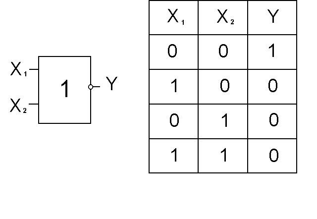

The Pierce element can be represented as a serial connection of the “OR” element and the “NOT” element (Fig. 6), and the Schaeffer element - as a serial connection of the “AND” element and the “NOT” element (Fig. 7).
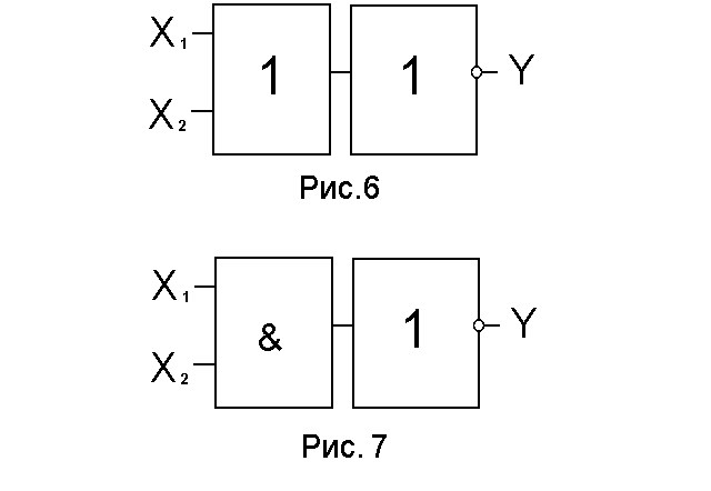
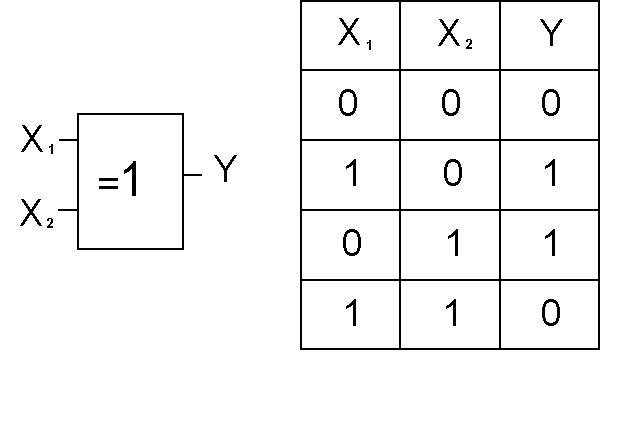
Fig.8 and Fig.9 show the elements “XOR” and “XOR - NOT”, realizing the functions of inequivalence and inequivalence with negation, respectively.

2.5. Logical elements that implement the operations of conjunction, disjunction, Pierce and Schaeffer functions can be, in general, n - input. So, for example, a logical element with three inputs that implements the Pierce function has the form shown in Fig. 10.
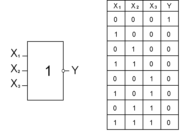
In the truth table (Fig. 10), in contrast to the tables in clause 2.4. there are eight values of the output variable Y. This number is determined by the number of possible combinations of input variables N, which, in general, is equal to: N = 2 n , where n is the number of input variables.
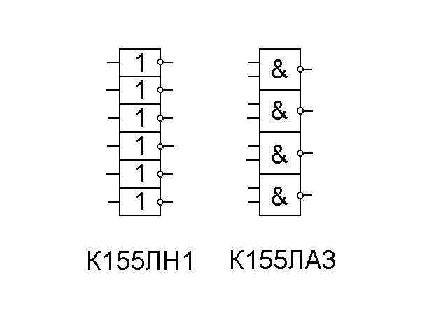
2.6. Logic elements are used to build integrated circuits that perform various logical and arithmetic operations and have different functional purposes. Microcircuits of the K155LN1 and K155LA3 types, for example, have six inverters and four Schaeffer elements, respectively (Fig. 11), and the K155LR1 microcircuit contains elements of various types (Fig. 12).
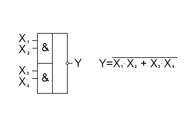
2.7. FAL of any complexity can be implemented using the specified logical elements. As an example, consider the FAL, given in algebraic form, in the form:
Simplify this FAL using the above rules. We get:
 (2)
(2)
The operation carried out is called FAL minimization and serves to facilitate the procedure for constructing a functional diagram of the corresponding digital device.
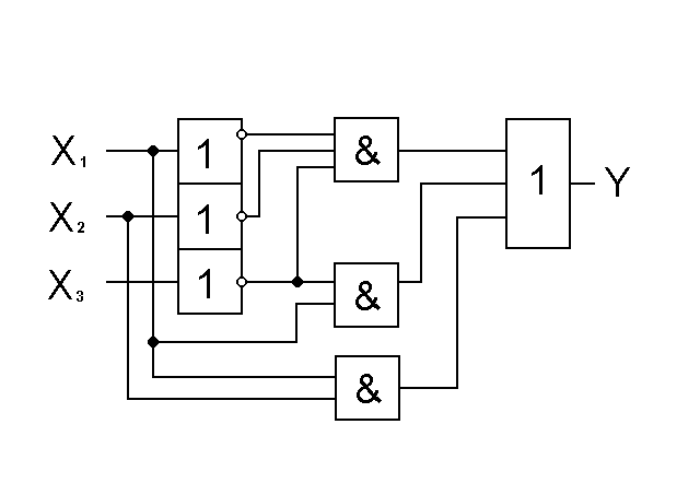
The functional diagram of the device that implements the considered FAL is shown in Fig.13.
It should be noted that the function (2) obtained after transformations is not completely minimized. Full minimization of the function is carried out in the course of the laboratory work.
3. Description of the object and means of research
The device studied in the laboratory work is shown in Fig.14.

3.1. The device is a group of logical elements made on K155 series microcircuits (elements DD1¸DD4).
For microcircuits of this series, the voltage U 1 \u003d (2.4 ¸ 5.0) V corresponds to a logical unit, and U 0 \u003d (0 ¸ 0.8) V corresponds to a logical zero.
3.2. Logic “0” and “1” at the input of the elements are set using the buttons located on the front panel of the K32 block under the inscription “Code programmer”. The numbers of the buttons on the panel correspond to the numbers on the device diagram.
The complete graphic representation of this type of pushbutton (so-called “latching pushbuttons”) is shown only for the SA1 pushbutton.
When the button is pressed, the input of the elements through the resistor R1 is connected to a source with a voltage of 5V. In this case, the voltage U 1 will act at the input of the elements, which corresponds to the supply of a logical unit to the output of the microcircuit. When the button is released, the input of the element will be connected to the bus, which is under the ground potential, which corresponds to applying a logical zero U 0 to the output of the microcircuit.
3.3. Logic signals from the outputs of the elements DD1 ¸ DD4 arrive at digital indicators and are induced in the form of symbols “0” and “1”. The digital indicators are located in block K32 on the left (“IO 2” button) under the indicators must be pressed.
3.4. The signal from the output of the DD5 element is fed through the switching circuits to the input of the H3014 multimeter. The multimeter is preliminarily set to the “-V” DC voltage measurement mode and the following connections are made:
3.4.1. The input - multimeter socket “-V” - is connected with a cable to the socket “Output V ~“ of block K32.
3.4.2. Socket XS1 on the board of the device is connected by a conductor to the left socket under the inscription “Input 1” in the field of the inscription “Switch”.
3.4.3. The “VSS VNK” button above the socket indicated above must be in the pressed state.
3.4.4. The “VKh 1” button under the inscription “Control V ~“ must be pressed, and the button “VVVNK” in the field of the inscription “KVU” must be in the depressed state.
4.1. Research of features of functioning of logical elements DD1 ¸ DD4 and definition of their functional purpose.
4.1.1. By setting various combinations of input logical signals, determine the value of the output signal and, based on the measurement results, fill in the truth tables for each element DD1 ¸ DD4 (Table 1 or Table 2, respectively) in the laboratory report.
Table 1.
Table 2.
4.1.2. Based on the measurement results (clause 4.1.1.), determine the functional purpose of the elements and put down their designation on the diagram in the laboratory report.
Attention! It is strictly forbidden to introduce designations into the text of the guidelines.
4.2. The study of the features of the functioning of the element DD5, the determination of its functional purpose and the measurement of voltage levels corresponding to the logical signals "0" and "1".
4.2.1. By setting the logical signals “0” and “1” using the SA12 button, at the input of the DD5 element, determine its functional purpose by the ratio of the output signals (see clause 3.1.). Measure the voltage value at the output of the element for each combination of input signals using a multimeter (clause 3.4.). Record the measurement data in a table.
Table 3
4.2.2. Based on the measurement results (clause 4.2.1.), determine the voltage levels of the logical zero U 0 and the logical unit U 1 for this type of microcircuit and establish their compliance with the passport data.
4.3. Carry out a complete minimization of the FAL, presented in clause 2.7. Based on the results of minimization, draw up a functional diagram of the device.
1. Title and purpose of the work
2. Scheme of the device under study
3. Tables 1,2,3
4. Results of measurements of U 0 and U 1 (clause 4.2.2.)
5. Formulas for calculation and calculation according to clause 4.3., device diagram
6. Conclusions on the work
6. Security questions
1. What values of variables does the algebra of logic operate on?
2. The main forms of the task of the FAL
3. Type of basic logic functions in algebraic form
4. What is a “logical element”?
5. What logical functions do the elements of Pierce and Schaeffer perform?
6. What determines the number of possible combinations of input variables for an arbitrary logic element?
7. List of used literature
Electrical engineering and fundamentals of electronics. O.A.Antonova, O.P.Gludkin et al., Ed. prof. O.P.Gludkina.-M.: Higher School, 1993.
SERGIEV POSAD
Lab #1
Logic functions, ELEMENTS and circuits
Objective
Study of logical functions, logic elements and circuits.
Devices and elements
Logic converter.
Word generator.
Voltmeter.
Logic probes.
Voltage source + 5 V.
The source of the "logic one" signal.
Two position switches.
Two-input elements AND, AND-NOT, OR, OR-NOT.
Microcircuits of the 74 series.
Brief information from the theory
Axioms of the algebra of logic
The variables considered in the algebra of logic can take only two values - 0 or 1. In the algebra of logic, an equivalence relation is defined (denoted by the sign =), the operation of addition (disjunction), denoted by the sign, multiplication (conjunction), denoted by the signs &, or a dot, and negations (or inversions), denoted by an underscore or an apostrophe."
The algebra of logic is defined by the following system of axioms:
x = 1 if x 0; x = 0 if x 1;
0&0 = 0; 1 1 = 1
1&1 = 1; 0 0 =0;
1&0 = 0&1 = 0; 0 1 = 1 0 = 1;
Boolean expressions
Logical expressions are usually written in conjunctive or disjunctive normal forms. In the disjunctive form, logical expressions are written as the logical sum of logical products, in the conjunctive form, as the logical product of logical sums. The procedure is the same as in ordinary algebraic expressions. Boolean expressions associate the value of a logical function with the values of boolean variables.
Logical laws and identities
When transforming logical expressions, the following logical laws and identities are used

Logic functions
Any logical expression composed of n variables using a finite number of logic algebra operations can be considered as some function of n variables. Such a function is called a logical function. In accordance with the axioms of the algebra of logic, the function can take on the value of 0 or 1, depending on the value of the variables. The function of n logical variables can be defined for 2 n values of variables corresponding to all possible values of n-bit binary numbers. The following functions of two variables x and at
f 1 (x, y) = x & y = x y = x - logical multiplication (conjunction),
f 2 (x, y) = x y - logical addition (disjunction),
f 3 (x,y) = = – Schaeffer stroke,
f 4 (x,y) = = – Pierce arrow,
f 5 (x,y) = x y = – addition modulo 2,
f 6 (x, y) = ![]() - equivalence.
- equivalence.
Logic
A physical device that implements one of the operations of the algebra of logic or the simplest logical function is called a logical element. A circuit composed of a finite number of logical elements according to certain rules is called a logical circuit. The main logical functions correspond to the circuit elements that perform them.
truth table
Since the domain of definition of any function of n variables is finite (2 n values), such a function can be defined by a table of values f(i), which it takes at points i, where i= 0,…,2 n -1. Such tables are called truth tables. Table 1 presents the truth tables that define the above functions.
Table 1
| Variable values | ||||||||
| x | at | f1 | f2 | f 3 | f4 | f5 | f6 | |
| 0 | 0 | 0 | 0 | 0 | 1 | 1 | 0 | 1 |
| 1 | 0 | 1 | 0 | 1 | 1 | 0 | 1 | 0 |
| 2 | 1 | 0 | 0 | 1 | 1 | 0 | 1 | 0 |
| 3 | 1 | 1 | 1 | 1 | 0 | 0 | 0 | 1 |
Karnot maps
If the number of logical variables does not exceed 5-6, it is convenient to transform logical equations using Karnaugh maps. The purpose of the transformations is to obtain a compact logical expression (minimization). Minimization is performed by combining neighboring sets (terms). The merged sets must have the same feature values (all 0's or all 1's). For clarity, consider an example: let it be required to find a logical expression for the majority function f m of three variables x, y, z, described by the truth table shown in Table 2.
table 2
Majority function
| № | x | y | z | f m |
| 0 | 0 | 0 | 0 | 0 |
| 1 | 0 | 0 | 1 | 0 |
| 2 | 0 | 1 | 0 | 0 |
| 3 | 0 | 1 | 1 | 1 |
| 4 | 1 | 0 | 0 | 0 |
| 5 | 1 | 0 | 1 | 1 |
| 6 | 1 | 1 | 0 | 1 |
| 7 | 1 | 1 | 1 | 1 |
Here the row number is equal to the number i= 2 2 x+2 1 y+2 0 z formed by the values of the variables.
Let's make a Karnot map. It is something similar to a table, in which the names of columns and rows represent the values of variables, and the variables are arranged in such an order that when moving to an adjacent column or row, the value of only one variable changes. For example, in row xy of Table 3, the values of the xy variables can be represented by the following sequences 00,01,11,10 or 00,10,11,01. The table is filled with function values corresponding to combinations of variable values. The resulting table looks like the one shown below (Table 3).
Table 3
Carnot Map
majority function
xy  z z | 00 | 01 | 11 | 10 |
| 0 | 0 | 0 | 1 | 0 |
| 1 | 0 | 1 | 1 | 1 |
On the Karnaugh map, we mark groups consisting of 2 k neighboring cells (2,4,8,) and containing 1, since they are described by simple logical expressions. Three ovals in the table define the logical expressions xy, xz, yz. Each oval joining two cells corresponds to logical transformations:

A compact expression describing a function is a disjunction of the logical expressions obtained with the help of Karn maps. As a result, we obtain an expression in disjunctive normal form
f m = xy v xz v yz .
If we combine 0, then we get the expression in conjunctive normal form
f m = (x v y)(x v z)(y v z).
When implementing the majority function of three logical variables, we obtain a circuit that, when three signals are applied to its inputs, will generate a signal at the output equal to the signal at most inputs (2 out of 3 or 3 out of 3). This scheme is used to restore the true value of the signals arriving at the 3 inputs, if an error is possible on one of the inputs.
To implement this function on the elements 2I-NOT, it is necessary to carry out the following transformations:
For DNF, a simpler expression is obtained, so it should be implemented. The corresponding circuit implementation is shown in fig. one.
 |
Rice. one
STUDY OF LOGIC ELEMENTS
transcript
1 16 The study of the logic of the work of logical elements Purpose of the work The purpose of the work is to consolidate knowledge of the basics of the algebra of logic and gain skills in the study of logical elements and connecting them into the simplest combinational circuits.
2 17 to 1. Information from the theory combinational circuits consist of logical elements. A logical element is the simplest part of a digital circuit that performs logical operations on logical variables. When using integrated circuits, such elements are usually elements of the AND-NOT, OR-NOT, AND-OR-NOT type. The work of logical elements is described by truth tables. On electrical functional diagrams, logical elements are displayed in the form of conventional graphic symbols (UGO). Conditional graphic designations of logical elements for two inputs are shown in Fig. 2.1a 2.1e. The truth tables for these elements have the form shown in Table NOT 2I 2OR 2I-NOT 1 1 a) b) c) d) e) element ab NOT 2AND 2OR 2AND-NOT 2OR-NOT Y = a Y = ab Y = avb Y = ab Y = avb line of the table in which the function Y takes the value "1", write down the logical product (conjunction) of the input variables (for table. 2.1, we mean variables a and b). Moreover, if the variable in this line takes the value "0", then in the conjunction it is written with inversion. Further, if necessary, the resulting function should be minimized.
3 18 2. Brief description of the laboratory setup A stand of the UM-11 type is used as a laboratory setup. The stand is based on a power supply, clock and single pulse generators, a set of logic elements and triggers, as well as display and control elements. The inputs and outputs of all elements are displayed on the front panel of the stand in the form of contact sockets. On the front panel of the stand there are conditional graphic designations of logical elements and triggers. With the help of special wires with tips, you can connect elements to each other, apply signals from generators or switches to the inputs of the elements, and also observe the signal values using indicator lights or using an oscilloscope. A fragment of the front panel of the stand is shown in Fig. Fig. Fragment of the panel of the UM-11 stand In addition to the elements for 2, 3 and 4 inputs shown in fig. 2.2, there is also an NAND element for 8 inputs on the front panel. Such a set of elements corresponds to a series of 155 integrated circuits. Thus, using the stand, you can assemble combinational circuits and check the correctness of their work.
4 19 3. Work order Task 1. Explore the logic of the 2I-NOT element. To do this, assemble the circuit shown in Fig. When constructing the circuit, use switches that can be used to send signals "0" and "1" to the input of the element. output signals to observe the status of the indicator light. When assembling the circuit, you should pay attention to the fact that each switch can set the value of one variable. In this case, the switch has two outputs: direct (upper) and inverse (lower). So from the top output of the switch you can get the direct value of the variable, and from the bottom the inverse value (Fig. 2.3). The direct value of the variable itself depends on the position of the switch: in the upper position of the switch, the variable is equal to "1", in the lower position "0". Accordingly, the inverse value will be reversed. Using the switches, apply all combinations of signals "a" and "b" to the input of the circuit and enter the obtained values of the output signals into the truth table. Compare the resulting table with the data in Table. 2.1.for the element 2I-NOT. Enter in the report: the assembled circuit, the UGO of the 2I-NOT element and the resulting truth table. +5V a1 a b Y 1 b To do this, assemble a circuit similar to the circuit in Fig. Check the logic of the circuit for various values of input signals and compile a truth table. Task 3. Explore the logic of the NOT element, implemented on the basis of the 2I-NOT element. To do this, assemble the circuit shown in Fig. 2.4. and complete it with a switch and an indicator light. Fig Implementation of the NOT circuit on 2I-NOT elements
5 20 Check the logic of the circuit for different values of the input signal and compare it with the data in Table. 2.1 for the NOT element. Task 4. Assemble the circuit shown in fig. 2.5 and explore the logic of its operation. Make a truth table and compare it with the data in Table. 2.1 for element 2I. Fig Scheme of the implementation of the circuit AND on the elements of AND-NOT Task 5. Assemble the circuit shown in Fig. 2.6 and examine the logic of its operation. Make a truth table and compare it with the data in Table. 2.1 for element 2OR. Fig Scheme of the implementation of the OR circuit on the elements of AND-NOT Task 6. Assemble the circuit shown in fig. 2.7 and explore the logic of its operation. Make a truth table and compare it with the truth table for the element 2AND-2OR. Fig An example of a scheme based on NAND elements 4. Contents of the report 1. Theme, purpose of the work, 2. The results of the assignments. For each task, bring the scheme of the experiment, the UGO of the element under study and the truth table. 3. Analysis of the obtained results. 4. Conclusions on the work.
6 21 5. Test questions 1. What is a logical function? 2. What is a logic element? 3. Explain the logic of the NOT element. 4. Explain the logic of the AND element. 5. Explain the logic of the OR element. 6. Explain the logic of the AND-NOT element. 7. Explain the logic of the OR-NOT element. 8. What is a truth table? 9. How to write a logical function in SDNF according to the truth table? 10. How to build a NOT circuit from AND-NOT elements? 11. How to build an AND circuit from AND-NOT elements? 12. How to build an OR circuit from AND-NOT elements? 13. What function does the circuit shown in fig. 2.7.
23 1. General information about combinational circuits Combination circuits consist of logical elements. When using integrated circuits, such elements are usually elements of the type AND-NOT, OR-NOT,
Laboratory work 8 Simulation of the simplest logical circuits The purpose of the work is the modeling of logical functions using logic elements. Work assignment Homework. In accordance with the given
Purpose of the program 34 1. Brief description of the program
Ministry of Education and Science of the Russian Federation Ural Federal University named after the first President of Russia B.N. Yeltsin LOGIC ELEMENTS ON INTEGRATED MICROSCHEMS Guidelines
Laboratory work 10 Modeling triggers and registers The purpose of the work is to acquire practical skills in building and researching various types of triggers and registers. Work assignment 1 Homework
Work 8. Research of multiplexers The purpose of the work: the study of the principles of construction, practical application and experimental research of multiplexers Duration of work 4 hours. Independent
Practical work 1 Analysis and synthesis of logical and relay control systems
Ministry of Education and Science and the Russian Federation Federal Autonomous Educational Institution of Higher Education SOUTHERN FEDERAL UNIVERSITY Institute of Nanotechnology, Electronics and Instrument Engineering
Name of the test: Circuit Engineering Intended for students of the specialty: spec. INTERNAL Text of the question 1 Define the concept symbol 2 Define the concept code
Work RESEARCH OF DECODERS Purpose of work: study of the principles of construction and methods of synthesis of decoders; prototyping and experimental study of decoders In the process of self-preparation
Work 1 Research of operation of logical elements 1. Purpose of work The purpose of the work is to study the principle of operation of digital logic elements (LE). 2. Guidelines 2.1. LE and logical operation
Federal State Autonomous Educational Institution of Higher Education "National Research University "Higher School of Economics" Faculty: Moscow Institute of Electronics and Mathematics
Kazan State Technical University A.N. Tupoleva Department of radio-electronic and telecommunication systems Shcherbakova TF, Kultynov Yu.I. Combination and serial nodes of digital
Job. SYNCHRONOUS TWO-STAGE TRIGGERS The purpose of the work is to study the principles of construction and circuits, static and dynamic modes of operation of synchronous two-stage triggers. Hours of work..structure
Lecture 5 Synthesis of combinational circuits on decoders Definition and classification A decoder is a combinational device that generally converts one type of binary code to another. Most
LABORATORY WORK 4 "Investigation of the work of Encoders and Decoders" 1 Purpose of the work: 1.1 Familiarization with the main characteristics of integral code converters: decoders, encoders. 2 Literature:
MINISTRY OF EDUCATION OF THE RUSSIAN FEDERATION MOSCOW ENERGY INSTITUTE (TECHNICAL UNIVERSITY) A.T. KOBYAK TRIGGERS Manual for laboratory work MOSCOW 2004 TRIGGERS Trigger
Methodological guide for students in computer science Topic 1. Forms of representation of logical functions (perfect disjunctive and conjunctive normal forms) Appendix 2.19.5 If the logical function is presented
222 Laboratory work 13 Synthesis and simulation of the code converter 1. The purpose of the work To master the procedure for the synthesis and simulation of the code converter using the Multisim 11.0.2 program. 2. General information
Laboratory work 1 Computer digital logic. 1. The purpose of the work The purpose of the work is to study the logical elements of the computer and their truth tables, as well as the construction of triggers in the Logisim program.
The study of the KLA7 logic circuit The purpose of the work is to study the device and the principle of operation of the KLA7 logic circuit. General Information The KLA7 integrated circuit contains an NAND element built on CMOS structures.
"LOGIKA-M" Training and laboratory stand Technical description and operating instructions Contents page 1. Purpose... 2 2. Specifications... 2 3. Design of the stand... 3 4. Laboratory work
TASKS AND METHODOLOGICAL INSTRUCTIONS for the implementation of the test on the discipline "Elements of automation systems" by students of the correspondence faculty Direction of preparation 000-Electric power and electrical engineering
Solving problems using conjunctive normal and disjunctive normal forms Elena Evgenievna Lapsheva, PRCNT SSU, Saratov Physico-Technical Lyceum February 6, 2007
Ministry of Education and Science of the Russian Federation Federal Agency for Education Saratov State Technical University REGISTER RESEARCH Guidelines for implementation
3. Elements of circuitry. Logic circuits Objectives: - to get acquainted with the elements and principles of building logical circuits; - consolidate the understanding of the basic laws of the algebra of logic; - learn to simplify logical
Control and evaluation tools for current control according to MDK.01.01 Digital circuitry (2nd year, semester 2018-2019 academic year) Current control 1 Control form: Practical work (Survey) Descriptive
FEDERAL RAILWAY TRANSPORT AGENCY Federal State Budgetary Educational Institution of Higher Professional Education "MOSCOW STATE UNIVERSITY OF TRANSPORT"
MINISTRY OF EDUCATION AND SCIENCE of the Russian Federation R.E.
LABORATORY WORK 1 SYNTHESIS OF COMBINATION DEVICES ACCORDING TO A GIVEN LOGIC FUNCTION Purpose of the work: 1. Study of methods for synthesizing combinational devices according to a given logical function. 2. Construction of combinational
Laboratory work 9 Simulation of combinational devices The purpose of the work is to study the forms of representation of numbers in digital devices and to study the circuits of combinational digital devices of decoders, multiplexers
FEDERAL AGENCY FOR EDUCATION STATE EDUCATIONAL INSTITUTION OF HIGHER PROFESSIONAL EDUCATION "VORONEZH STATE UNIVERSITY" LOGICAL ELEMENTS Guidelines
Logical models of switching circuits Information processing Physical principle of information processing The information to be converted is encoded by a sequence of pulses, the processing of which takes place
Job. Synchronous single-stage triggers with static and dynamic recording control
Laboratory work 11 Simulation of impulse counters The purpose of the work is to study the structure and study the operation of adding and subtracting binary counters, as well as counters with a conversion factor that is different
Laboratory work 2. Triggers Purpose: To study the purpose and principle of operation of trigger devices. Introduction to basic trigger devices from the EWB library. Equipment: Electronic Lab Electronics
ELEMENTS OF AUTOMATIC SYSTEMS Topic 2 Logic circuits and their minimization I.V. Muzylev 23 Basic concepts of the algebra of logic http://cifra.studentmiv.ru Logic circuits Compilation of truth tables for logical
4. LABORATORY WORK 3 RS AND D-TRIGGER The purpose of the lesson: building and familiarizing with the operation of the main circuits of RS and D flip-flops using the tools of the digital part of the EWB package, consolidating the theoretical
1. PURPOSE OF THE WORK 1.1. To study the functional and electrical characteristics of the ALU on the IC K155 IP3. 1.2. Obtain practical skills in researching the operation of ALU ICs by applying inputs, observing
1. PURPOSE OF THE WORK 1.1. To study the functional and electrical characteristics of the decoders on the IC K 155 ID4; K 155 ID7; 1.2. Get practical skills in researching the operation of decoder ICs by submitting
Topic 4. Logical foundations of computers 1. BASIC INFORMATION FROM THE ALGEBRA OF LOGIC ... 1 2. LAWS OF THE ALGEBRA OF LOGIC ... 4 3. THE CONCEPT OF MINIMIZATION OF LOGICAL FUNCTIONS ... 6 4. TECHNICAL INTERPRETATION OF LOGICAL FUNCTIONS ...
Direction 09.03.03 Informatics 1.2 Lecture "Logical foundations of informatics" Lecturer Molnina Elena Vladimirovna Senior lecturer of the Department of Information systems, room 9, main building. mail: [email protected]
LABORATORY WORK STUDY OF ELECTRIC PROCESSES IN SIMPLE LINEAR CIRCUITS The purpose of the work: to study the transfer coefficient and phase shift between current and voltage in circuits consisting of series
Control task Depending on the issued version, you need to build a CLS of a decoder, encoder, multiplexer or adder. Option 7 to decimal: "7" 7 "7" 7 0 0 0 0 0 0 0 5 0 0 0 0 0
Amendment and you have every chance to learn to understand people. As a result of the study, it was revealed that most of the students use sign language and partially understand the meaning of body movements.
3 Lecture 3. COMBINATION DIGITAL DEVICES Plan. Encoders, decoders and code converters. Multiplexers and demultiplexers. 3. Adders.. Conclusions.. Encoders, decoders and converters
Electronics and MPT Synthesis of logical circuits according to a given function Representation of logical functions (LF) 3 ways of representing logical functions:. graph (in the form of a voltage time diagram); 2. analytical
STUDY OF ELEMENTARY LOGIC ELEMENTS Guidelines Ulyanovsk 2006 1 Federal Agency for Education State educational institution of higher professional education
Ministry of Education and Science of the Russian Federation Federal State Autonomous Educational Institution of Higher Professional Education Kazan (Volga Region) Federal University
LABORATORY WORK "FUNDAMENTALS OF DIGITAL TECHNOLOGY" Fig. 1. General view of the laboratory stand 1 Work 1 STUDY OF RECTANGULAR PULSES GENERATORS 1. Purpose of work Familiarization with the main functions and testing
MINISTRY OF STUDIES AND SCIENCES OF UKRAINE NATIONAL METALLURGICAL ACADEMY OF UKRAINE METHODOLOGICAL EXPOSURE TO VISOKANNYA LABORITORY ROBIT AND PARTICULAR WORK IN THE DISCIPLINE "COMP UTTERIV ARCHITECTURE" FOR STUDENTS
MINISTRY OF TRANSPORT OF THE RUSSIAN FEDERATION STATE CIVIL AVIATION SERVICE MOSCOW STATE TECHNICAL UNIVERSITY OF CIVIL AVIATION Department of Computers, Complexes, Systems and Networks Coursework
(basic concepts - compilation of complex expressions - truth tables - laws of propositional logic - examples) The initial concept of propositional logic is a simple or elementary proposition. This
Laboratory work 3 Schemes on D-flip-flops Department of the Sun SibGUTI 2012 Contents 1. Objectives of the work: ... 3 2. Trigger in counting mode ... 3 3. Divider ... 3 4. Description of microcircuits K176TM1 and K176TM2 ... 4 5.
ARCHITECTURE OF COMPUTERS AND COMPUTING SYSTEMS Lecture 3. Logical foundations of computers, elements and nodes. Lecturer Tsveloy Vladimir Andreevich PURPOSE: TO STUDY THE BASIC OPERATIONS OF THE ALGEBRA OF LOGIC, THE BASIS OF CONSTRUCTING COMBINATIONAL
Chapter 3 LOGIC AND LOGICAL FOUNDATIONS OF THE COMPUTER 3.1. Algebra of logic The first teachings about the forms and methods of reasoning arose in the countries of the Ancient East (China, India), but modern logic is based on
1 The simplest information converters Mathematical logic with the development of computers turned out to be in close relationship with computational mathematics, with all issues of design and programming
1. PURPOSE OF THE WORK 1.1. To study the functional and electrical characteristics of semiconductor ROMs on ICs K155PR6, K155PR7. 1.2. Get practical skills in researching the operation of IC ROM K155PR6, K155PR7
Contents Preface 14 Chapter 1. Digital systems and presentation of information 19 1.1. Digital systems 19 1.1.1. Control systems 20 Logic signals and functions 21 Positive and negative logic
Ministry of Education and Science of the Russian Federation Federal State Budgetary Educational Institution of Higher Professional Education Nizhny Novgorod State Technical University. R.E.
A.I. Nedashkovsky Laboratory work Asynchronous and synchronous pulse counters The purpose of the work is knowledge of the construction structures, parameters and modes of operation of pulse counters, the ability to analyze their work,
Ministry of Education of the Russian Federation ORENBURG STATE UNIVERSITY Department of Instrument Engineering E. A. Kornev
Open lesson “Construction of logic circuits. Basic logical elements". Type of lesson: combined (testing students' knowledge, learning new material). Class: 10 A class Date: 17.01.2009
Laboratory work 2. Research of work of triggers. Department of the Armed Forces SibGUTI 2012 Contents 1. The purpose of the work: ... 3 2. General information ... 3 3. Asynchronous RS-trigger ... 4 4. Synchronous single-stage D-trigger ....
PROCEDURE OF PERFORMING WORK Task for work To measure vibrations at installation of the car without shock-absorbers and with shock-absorbers. Based on the measurement results, determine the effectiveness of the vibration isolation of the machine. In complicated
Lab #2
Literature:
2. V.S. Yampolsky Fundamentals of automation and EVT. – M.: Enlightenment. - 1991. - §3.1 -3.4
Working process:
- Turn on the terminal, connect to the local network and download the Fundamentals of Microelectronics website. Select the number of the laboratory work, register and proceed with the assignments according to the instructions that appear on the screen and this description.
- In each of the 10 tasks, select a node containing only logical elements from the above diagram of a digital machine and depict its circuit diagram using the UGO of the Russian standard
- Simulate the operation of each circuit using Electronic Workbench and compile a truth table of the device under study
- Determine the logical function of the device under study and bring its conditional graphic image (UGO)
- In each task, create two additional schemes for implementing the same logical function on 2AND-NOT elements (Schaffer element) and 2OR-NOT elements (Pierce element), using the minimum number of gates
- In task 11, by analogy with the previous diagrams, supplement the above device with a diagram of a node that allows you to apply an arbitrary combination of logical signals to the inputs X1-X3 and indicate the state of each input and output. Explore the operation of the circuit in the same way as the previous tasks
A report for each task of laboratory work should be drawn up according to the model given in APPENDIX 1.
When defending a work, be able to explain each of the results obtained.
ATTACHMENT 1
Fragment of the report (on the example of one task)
Exercise 1.
An example of the scheme given in the assignment.
IN this way redraw it no need!
A fragment of the report on this assignment is given below.
Task 1: the function performed by the circuit - "2I-NOT"
Scheme: UGO: Truth table:


"2I-NOT" on Schaeffer's elements. "2I-NOT" on Pierce's elements.


APPENDIX 2
UGO and truth tables of some logic elements
1. Element "2I-NOT"


2. Element "2OR-NOT"


3. XOR element


APPENDIX 3
Examples of conventional graphic symbols for logical elements according to GOST (Russian standard) and ANSI (American National Standard Institute)
| UGO by ANSI | UGO according to GOST | Functional purpose |
| "2I" (2-Input AND Gate) | ||
| "3I" (3-Input AND Gate) | ||
| "2I-NOT" (2-Input NAND Gate) | ||
| "2OR" (2-Input OR Gate) | ||
| "2OR-NOT" (2-Input NOR Gate) | ||
| "3OR-NOT" (3-Input NOR Gate) | ||
| "NOT" (NOT Gate) | ||
 | "XOR" (2-Input XOR Gate) | |
| "XOR-NOT" (2-Input XNOR Gate) | ||
| 6-Input Modulo 2 Adder (6-Input XOR Gate) |
Laboratory work number 3.
Study of RS-, RST-, D- and JK-type triggers.
Literature:
1. A.A. Kovalenko, M.D. Petropavlovsky. Fundamentals of microelectronics: Textbook. - Barnaul: Publishing house of BSPU, 2005. - 222 p.
2. V.S. Yampolsky. Fundamentals of automation and electronic computing technology. – M.: Enlightenment. - 1991. - 223 p.
4. Guide to Performing Virtual Labs with Electronic Workbench 5.12 Electrical Simulator
Working process:
- Turn on the terminal, connect to the local network and download the Fundamentals of Microelectronics website. Select the number of the laboratory work, register and proceed with the tasks according to the instructions that appear on the screen and this description
- Explore the operation of an asynchronous RS flip-flop with inverse inputs on 2I-NOT logic elements.
Using the Electronics Workbench program, assemble the trigger circuit shown in the figure.

To control the trigger, use the switches (Switch) that connect the inputs to the power plus terminal (V cc) or to the ground terminal (Ground), and to indicate the status of the inputs and outputs, use probes (Green Probe and Red Probe, respectively).
Conduct research in the following order:
Trigger state table
| Combination No. | Operation | ||
| Output setting | |||
In an abbreviated version, the state table of an RS flip-flop with inverted inputs is usually depicted in the following form (with a given combination of input signals, the output Q is set to the specified state regardless of its previous state):
 Here, the symbol (t + 1) means the state of the trigger "in the next cycle", i.e. after setting the output according to the input signals
Note: (in this and other similar tables, the following designations are adopted):
- Explore the operation of an asynchronous RS flip-flop with direct inputs on 2I-NOT logic elements.
 To do this, add 2 more 2I-NOT elements to the assembled circuit to get a trigger with direct inputs (see figure), and based on the experiment in the Electronics Workbench environment, by analogy with the previous task, fill in the table of its states
- Explore the operation of a synchronized RS flip-flop (RST flip-flop).
 |
To do this, open the RST flip-flop circuit (file E:\MeLabs\Lab3\rst_trig_analis.EWB), to the inputs of which a Word Generator is connected, and all input and output signals are controlled by the Logic Analyzer. Expand the word generator panel and set its Step mode. Enter into the memory of the generator the hexadecimal codes of the words of your variant. Expand the logic analyzer panel. Turn on the simulation and, sequentially pressing the LMB on the “Step” button located on the word generator panel, generate the entire test sequence. Sketch the diagrams obtained by the logic analyzer in your notebook. Fill in the cycle-wise trigger state table.
Trigger state table
| Information signal | Bar numbers | |||||||||
| C | ||||||||||
| R | ||||||||||
| S | ||||||||||
| Q |
- Explore static and dynamic D-flip-flops. Open the scheme of parallel-connected static and dynamic D-triggers (file E:\MeLabs\Lab3\D_trig.EWB), to the inputs of which a Word Generator is connected, and all input and output signals are controlled by probes.
 |
Expand the word generator panel. From the state table, write out the binary codes of words by cycles and, converting them to 16, enter them into the memory of the word generator. Turn on the simulation and, sequentially pressing the LMB on the “Step” button located on the word generator panel, generate the entire test sequence. Fill in the cycle-wise table of trigger states.
Trigger State Table
| Information signal | Bar numbers | |||||||||
| C | ||||||||||
| D | ||||||||||
| Q stat. | ||||||||||
| Q dyn. |
- Open the JK flip-flop schema with dynamic control (jk_trig_analysis).
 |
Expand the word generator panel and set its Step mode. Enter into the memory of the generator the hexadecimal codes of the words of your variant. Turn on the simulation and, sequentially pressing the LMB on the “Step” button located on the word generator panel, generate the entire test sequence. Sketch the diagrams obtained by the logic analyzer in your notebook. Fill in the cycle-wise trigger state table.
Trigger state table
| Information signal | Bar numbers | |||||||||||
| C | ||||||||||||
| J | ||||||||||||
| K | ||||||||||||
| Pre | ||||||||||||
| Clr | ||||||||||||
| Q |
Note: Unlike the previously studied circuits, this task examines the operation of a specific 7476 chip (Dual JK MS‑SLV FF (pre, clr)), and therefore, when simulating, it is necessary to connect the Vcc power supply and the GND ground to the corresponding pins. The task uses the outputs of only one of the JK flip-flops (the first one). Inputs Pre (preset) and Clr (clear) play the role of setting inputs S and R, respectively.
- Choose from the library Digital JK flip-flop IC 7472 (And-gated JK MS-SLV FF (pre, clr)) and assemble the counting flip-flop circuit on it. Please note that 3I logic is used at the information inputs. The NC pin of the microcircuit is free (not used).
 Apply to the input of the trigger unipolar amplitude 5 V rectangular pulses from the function generator of the required frequency, get oscillograms of the input and output signals. Show them to your teacher.
